
DCM1000 DC-JVL Measurement System
View the recent news release: TOYOTech, Sharp Display Technology Corporation, and the Japan Advanced Institute of Science and Technology Develop an Innovative Measurement Technology to study OLED Behavior under Extremely Low Luminance Conditions
INTRODUCTION
Current density-Voltage-Luminance (JVL) measurements are widely used to evaluate organic light-emitting diodes (OLEDs). These measurement results are mainly discussed about current density and luminance in high-voltage regions. However, it has been required to evaluate JVL characteristics in a low driving voltage region to investigate behaviors such as charge injections and emissions in OLEDs.
DCM1000 is developed with Sharp Display Technology Corporation and Japan Advanced Institute of Science Technology (JAIST) for evaluations of OLEDs to obtain Displacement current-JVL (DC-JVL) data with high measurement sensitivity. The results provide a novel analysis approach of degradation for the OLED industry.
FEATURES
- Simultaneous measurement of DC-JVL
- Seamless measurements by optimizing the measurement range of current density and luminance
- Extremely high sensitivity and wide measurement range
- Various measurements and analysis
- Displacement current and current density vs. Voltage
- Luminance vs. Voltage
- Luminance vs. Current density
- Current efficiency vs. Current density
- Charge injection voltages
- OLED emission voltage
- Gap measurement between charge injection voltage and OLED emission voltage
- Charge amount measurement that does not contribute to OLED emission
- Resistance and capacitance measurement in displacement current region
MEASUREMENT PRINCIPLE
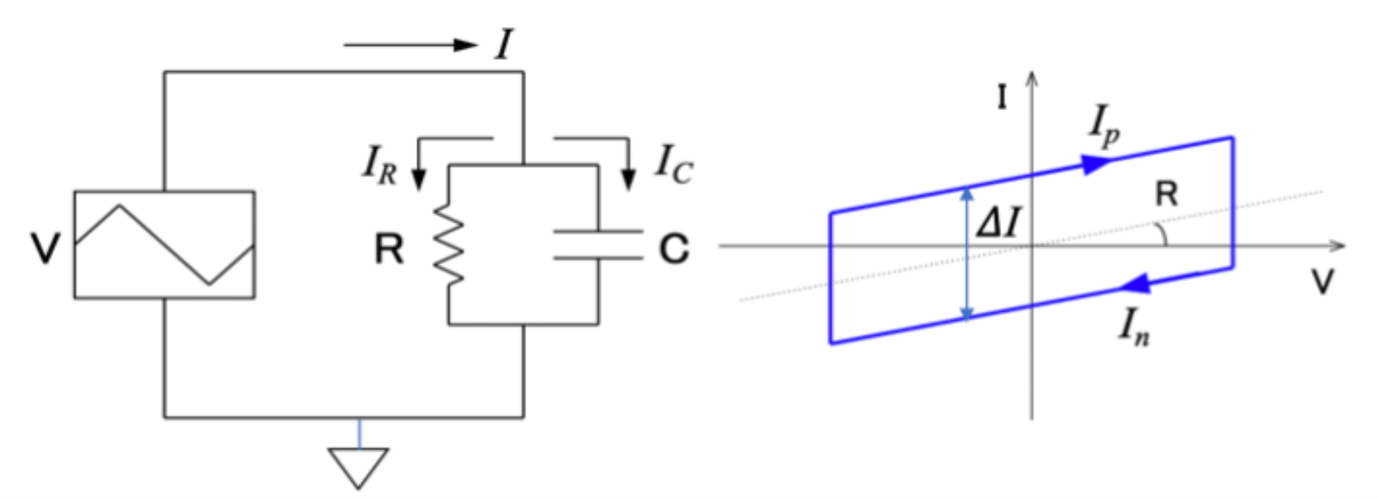
(a) Equivalent circuit (b) Current vs. Voltage characteristics
Figure 1: Displacement Current Measurement
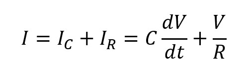
Figure 1 (a) shows the equivalent circuit of a displacement current measurement (DCM) for a capacitance and a resistance (CR) sample which are connected in parallel. A Triangular waveform voltage is applied to a CR sample, and the current vs. voltage characteristics are obtained as shown in Figure 1 (b). The total current (I) flowing through a capacitance (IC) and a resistance (IR) is define by:
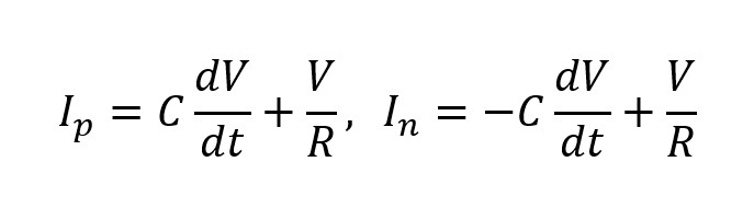
In case of dV/dt > 0 and dv/dt <0, the currents of a positive slope (Ip) and a negative slope (In) become:
Thus, the difference between Ip and In is proportional to the capacitance as follows:
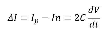

Figure 2: Equivalent Measurement Circuit of DCM1000
Figure 2 shows the equivalent measurement circuit of DCM1000 which can obtain displacement current and current density-voltage-luminance (DC-JVL) characteristics for OLEDs. A triangular waveform voltage is applied to an anode of an OLED sample and a current is measured from a cathode by using the current-to-voltage (I/V) converter to obtain a displacement current and a current density as a function of applied voltage (DC-JV). An EL intensity is measured by using a photodiode and the I/V converter. Each I/V converter has several feedback resistances so that the current range is automatically optimized to obtain a current. DCM1000 usually applies a low frequency triangle waveform which is 0.01 or 0.001 Hz to obtain a stable result. EL intensity is converted to luminance using the ratio of the EL intensity to the luminance on a defined voltage with a luminance meter. Note that DCM1000 provides relative luminance data for comparison, not absolute luminance data.
MEASUREMENTS
DCM1000 has many measurement functions for OLEDs as follows.
4-1. Displacement current measurement (DCM)1)
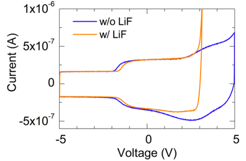
Figure 3: DCM Characteristics with and w/o LiF Layer
Figure 3 shows the measurement result of DCM of OLEDs which have α-NPD/Alq3/TPBi with and without a LiF layer. No significant difference of positive and negative currents between -5 V and -2 V for both OLEDs was observed, while both currents start to increase at -2.2 V and -1.8 V without and with a LiF layer, respectively. We found that the hole injection from an ITO layer to an α-NPD layer started around -2 V, and the LiF contributed to the reduction of the hole injection voltage by means of an increment of injection barrier. Further, the current of OLED with a LiF layer drastically increased from +3 V, while the current of OLED without the LiF showed a bump between +2 V and +4.5 V, and increased at +5 V. It is obviously suggested that the LiF contributed to the reduction of the electron injection voltage from +5 V to +3 V, having efficient electron injection characteristics. Regarding the bump of OLED without a LiF layer, we suppose that this can be ascribed to the hole injection from an α-NPD layer to an Alq3 layer before starting the electron injection from an Al layer to a TPBi layer. In case of the negative slope, the current peak was observed between +4 V and 0 V in OLED without a LiF layer. We suppose that this is related to the discharge of holes from the interface between an Alq3 layer and a TPBi layer. We also obtained the capacitance of OLEDs from the current difference at -3 V, resulting in 0.843 nF.
4-2. Comparison between conventional JV and DC-JV2)
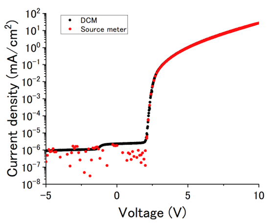
Figure 4: Conventional JV (Source meter) vs. DC-JV (DCM1000)
Figure 4 shows the comparison measurement results between conventional JV (Source meter) and DC-JV (DCM1000) for the α-NPD/Alq3 OLED sample. There was good agreement of each measurement results from +2 V to +10 V due to high current density. However, the conventional JV was not stable because of the limited sensitivity. We confirmed that DCM1000 can see charge injection behaviors in OLED with high sensitivity.
4-3. Sensitivity of photodiode3)
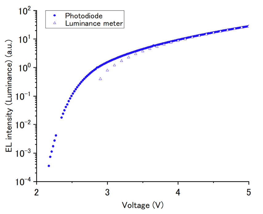
Figure 5: Comparison between Luminance Meter (BM-9) and Si Photodiode (DCM1000)
Figure 5 shows the comparison measurement results of EL intensity between the luminance meter (BM-9: Topcon) and the Si photodiode (DCM1000) for the α-NPD/Alq3 OLED sample. EL intensity was converted to luminance using the ratio of the EL intensity to the luminance on +5 V with the luminance meter. We found that the sensitivity of the conventional luminance meter was 10-1 cd/m2 and the results were derailed from the data of DCM1000 below +4V. On the other hand, the sensitivity of DCM1000 was 10-4 cd/m2 order, so we confirmed that DCM1000 has extremely higher measurement sensitivity than the conventional luminance meter.
4-4. Luminance vs. Current density3)
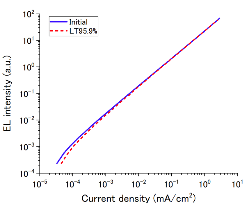
Figure 6: EL intensity (Luminance) vs. Current Density
Figure 6 shows the EL intensity (equivalent to Luminance) vs. Current density for the α-NPD/Alq3 OLED sample before/after degradation. The initial sample had a linear correlation of EL intensity and Current density and started to derail the linear correlation below 10-4 mA/cm2. However, the degraded sample started to derail the linear correlation below 10-2 mA/cm2. It is well known that luminance and current density should have a linear correlation, but DCM1000 could observe the non-linear correlation in low current density regions which may help to clarify the root cause of OLED degradations.
4-5. Conventional JV vs. DC-JV for OLEDs having EBL/EML/HBL4)

Figure 7: Current Density vs. Voltage for OLEDs
Figure 7 shows the current density vs. voltage characteristics of RGB OLED samples which have HIL/HTL/EBL/EML/HBL/ETL/EIL layers. The solid lines and the dots are the DC-JV which was the data of the first quadrant in the one-cycle measurement and the conventional JV characteristics, respectively. The results of the conventional JV characteristics were well-matched with those of DC-JV above 10-5 mA/cm2. Below 10-5 mA/cm2, the current density in the conventional JV characteristics of all OLED samples seems to overlap due to the limited current sensitivity of the source meter. On the contrary, the DC-JV characteristic shows a clear difference in current density below 10-5 mA/cm2. We observed that the onset voltages of the current change of red, green, and blue OLED samples were around 1.9 V, 2.0 V, and 2.3 V, respectively. We confirmed that the DC-JV measurement has higher sensitivity than the conventional JV.
4-6. Luminance vs. Voltage for OLEDs having EBL/EML/HBL4)
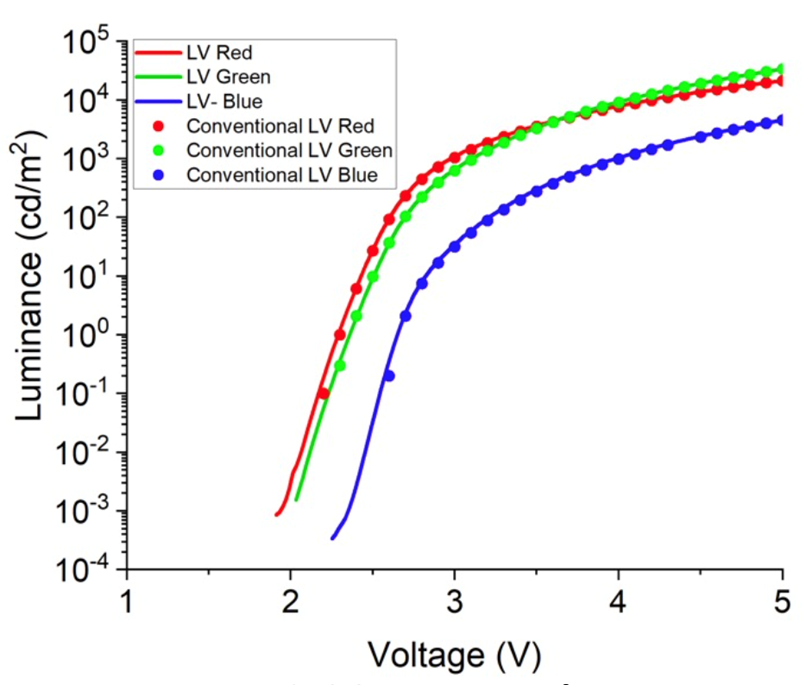
Figure 8: Luminance vs. Voltage for OLEDs
Figure 8 shows the luminance vs. voltage of OLEDs which are the same samples as Figure 7. The solid lines and the dots are the EL intensity which was converted to luminance and the luminance measured with a conventional luminance meter, respectively.
Both results were well-matched with the above 1 (cd/m2), but there were no data for the conventional luminance meter below 10-1 cd/m2 due to limitations of measurement sensitivity. Moreover, it seems that the data of the conventional luminance meter started to deviate from the data of the EL intensity around 1 – 10-1 cd/m2. On the other hand, the EL intensity measured by the photodiode was detected down to the order of 10-4 (cd/m2). We confirmed that the EL intensity measurement by using the photodiode could realize an extremely low luminance measurement.
4-7. Current efficiency vs. Current density for OLEDs having EBL/EML/HBL4)
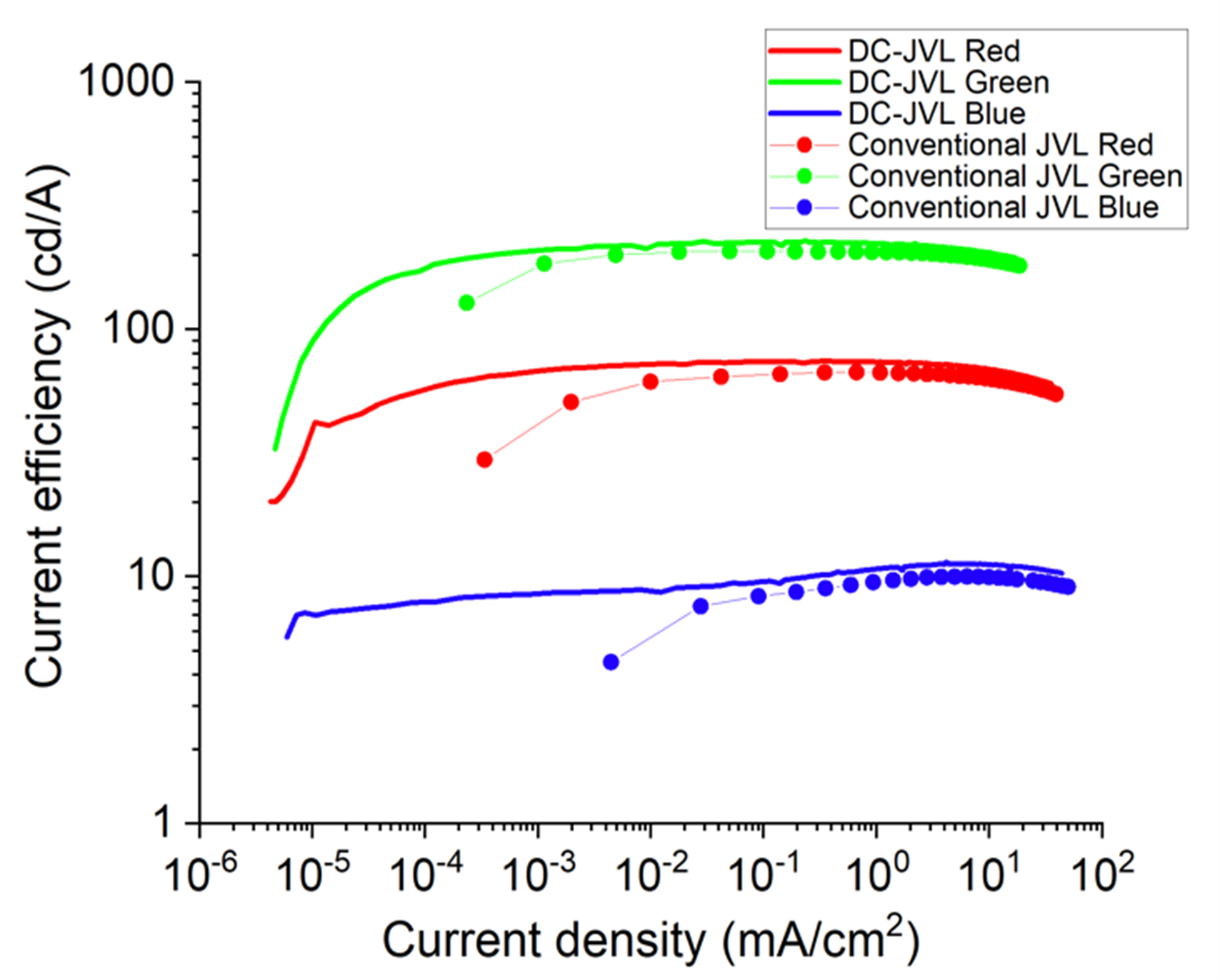
Figure 9: Current Efficiency vs. Current Density for OLEDs
Figure 9 shows the current density vs. current efficiency of OLEDs which are the same samples as Figure 7. The solid lines and dotted lines are the data of the DC- JVL measurement and the conventional JVL measurement, respectively. The current sensitivity of the DC-JVL measurement was in the order of 10-6 mA/cm2. On the other hand, the sensitivity of the conventional JVL was 10-4 to 10-3 mA/cm2 due to less sensitivity of the luminance meter, and the data deviated from that of DC-JVL at low current densities. We demonstrated that DC-JVL measurement has a higher sensitivity than that of conventional JVL measurement. At low current densities below 10-3 mA/cm2, the current efficiencies of the R and G OLEDs show a significant increase with increasing current density and become independent up to a current density of 101 mA/cm2. On the other hand, the blue OLED shows a relatively weak dependence on the current density over the entire current density range. This difference can only be revealed with our DC-JVL measurement.
4-8. Blue OLED degradation4)5)
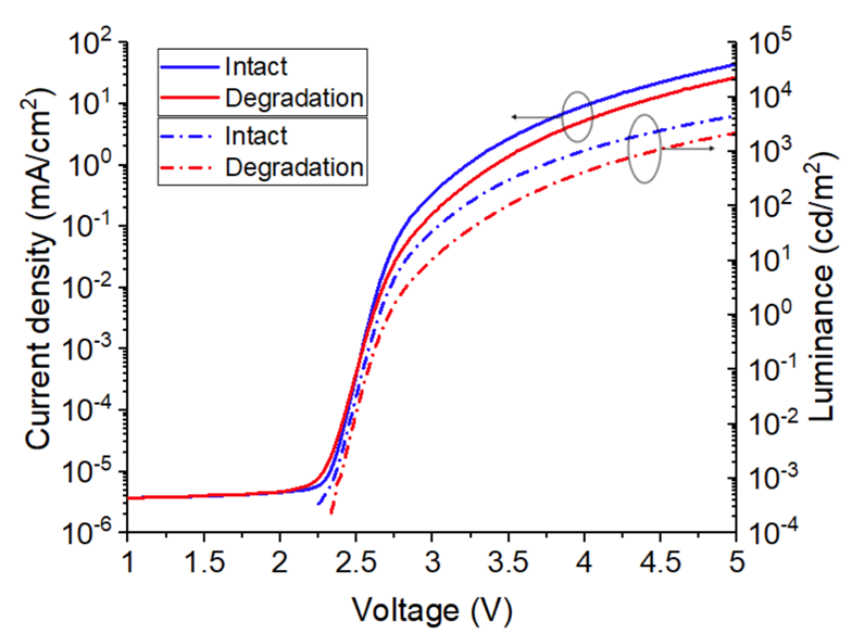
Figure 10: DC-JVL of Blue OLED before/after Degradation
Figure 10 shows the DC-JVL characteristics of blue OLEDs which are the intact and degraded pixels. We found that the current density and the luminance of the degraded pixel in the range between 2.5 V and 5.0 V became smaller than that of the initial pixel. We also found that the onset voltage of the current increase of the degraded pixel is smaller than that of the intact pixel. The results suggest that the onset voltage of the current increase of the degraded pixel started earlier than that of the intact pixel.

Figure 11: Magnified Data of Figure 10 (Linear Vertical Scale)
Figure 11 shows the magnified data of Figure 10 with a linear vertical scale to see the transitions of the current density and the luminance in detail. The charge injection of the initial and the degraded pixels started around 2.2 V and 2.0 V, respectively. On the other hand, the emission starting voltage of the degraded pixel was higher than that of the initial pixel. We confirmed that the order of luminance of the emission start was 10-4 cd/m2, which is extremely low luminance and hard to measure by conventional luminance meter. We also confirmed that the gap between the charge injection voltage and the emission start voltage of the initial pixel was 0.1 V. However, the gap voltage of the degraded pixel was about 0.3 V. We suppose that the gap between an onset voltage of current increase and an emission start voltage is related to the emission loss during charge injections(①) and emissions(②) as shown in Figure 12.
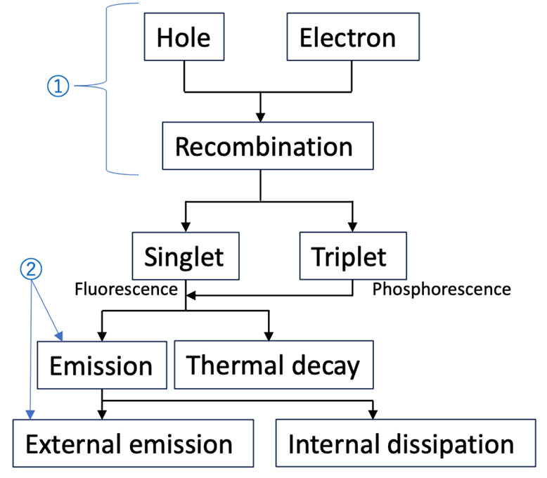
Figure 12: Process of Charge Injections and Emissions
4-9. Current efficiency vs. Current density for Blue OLED degradation4)
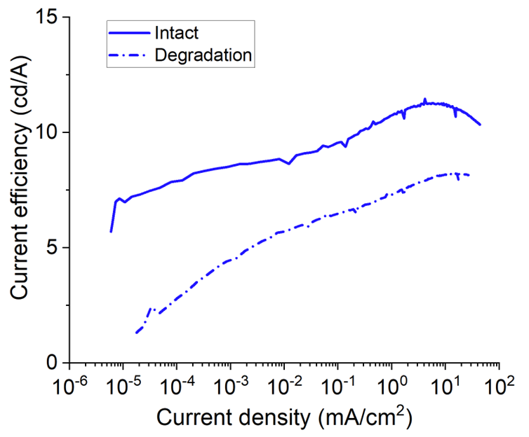
Figure 13: Current Efficiency of Blue OLED before/after Degradation
Figure 13 shows the current efficiency vs. current density of the blue OLED sample before and after degradation. The current efficiency of the intact pixel was gradually increased from 7 to 11 cd/A at a current density of 102 to 10-5 mA/cm2. The increase in current efficiency with increasing current density indicates that the operating mechanism of the blue OLED is based on a triplet-triplet fusion to generate the additional singlet exciton. The fact that the degraded pixel has a significantly lower current efficiency than the intact pixel suggests that the degradation of the blue OLED may be caused by the decrease in exciton generation efficiency and/or the quenching of the generated exciton.
SPECIFICATIONS |
|
| Frequency of triangle waveform | 1 mHz - 1 Hz |
| Voltage | ±10 V |
| Current density measurement range | 10⁻⁶ mA/cm² - 10² mA/cm² |
| Luminance range (not absolute value) | 10⁻⁴ cd/m² - 10⁵ cd/m² |
| Charge measurement | 1 pC ~ |
| Dimensions | 430 mm (W) x 133 mm (H) x 330 mm (D) |
| Weight | 6.0 kg |
MEASUREMENT COMPARISONS

REFERENCES
- Inoue M, Kaneko Y, Fujimoto H, Miyazaki H, Adachi C. Evaluations of lithium-fluoride behavior in OLEDs by means of cyclic DCM method. Dig Tech Pap – SID Int Symp. 2020;51(1):2107–10.
- Inoue M. Oyabu N, Murata H. Evaluations of an OLED by Optimized Displacement Current Measurement (DCM) Method. 36th Japan OLED Forum. S5-3; 2023.
- Inoue M, Murata H. Simultaneous Measurements of Displacement Current and EL Intensity for OLEDs. 37th Japan OLED Forum. S2-3; 2023.
- Inoue M, Mizusaki M, Murata H. Comparison between Conventional JVL and DC-JVL Measurements for OLEDs. Dig Tech Pap – SID Int Symp. 2024;55(1):2226–22.
- Inoue M, Mizusaki M, Murata H High Sensitivity Measurements of Displacement Current and Luminance for OLEDs. 38th Japan OLED Forum. S3-2; 2024